Physical Address
304 North Cardinal St.
Dorchester Center, MA 02124
Physical Address
304 North Cardinal St.
Dorchester Center, MA 02124
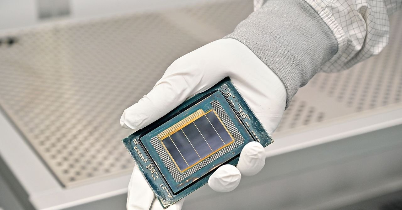
Four years later About construction, Intel said on Thursday that its fab 52 Semiconductor In Chandler, Arizona is now turning its first chips. The company also shared more details about the long-awaited CPU, which will produce the convenience using Intel’s brand-new 18 process technology.
This announcement comes just six weeks after the Trump administration Achieved a 9.9 percent partnership Intel exchange $ 8.9 billion stock. FAB Opening, Long in the Works, the first major opportunity to explain the broad technology industry for the struggling US chipmaker, which can make a number of advanced chips in the world – and the White House investment may stop.
Late last month, Intel invited a few dozen analysts and business partners to visit FAB 52 with a handful of journalists. This tour gives a very rare flash in the world Modern chipmeckingWhere robots perform most of the work, lithography machines print microscopic patterns on silicon weapers in the size of the school buses, and workers roam the opposition “bony suit,” booties, goggles and gloves. (Guests also have to wear a suit.) Intel is recycled in the fab every six seconds.
All of this is to prevent pollution of the whole computing industry that is driven by the fragile silicone weeer. If any of the specs landed on a wellfare, it could be irreparable damaged.
Intel says its fab has been technically operating since July 52 and the new generation of chips are being created, known as Panther Lake and Clearwater Forest, this time has been underway for years.
However, Intel has decided to display its new fab at an important moment for the company. This facility is designed to create chips using a new process called 18A, it is supposed to produce more powerful and efficient products. “Assuming” key topic: Intel’s close-fourth fate is just impressive enough to serve its ordinary hardware and computer customers, but it hangs on whether to produce a lot of cash with a lot of cash to spend on advanced chips and data centers.
During the tour, Intel Executives emphasized that Fab 52 is the most advanced chip production center in the world. This may be technically true – the company’s fiction or foundries, “long known and honored in the industry to make the next node possible,” Austin Lyons, analyst of creative techniques, says the founder of the semiconductor publishing chipstrat. For example, in the early 20’s, when the Intel 32-nanometer chip technology was launched, another significant node was created or the process was progressed when it introduced 32-nanometer chip technology. (Its latest chips 2-nanometers)